Phone: +86-755-2357-1819 Mobile: +86-185-7640-5228 Email: sales@ominipcba.com whatsapp: +8618576405228

BGA Assembly Explained: A Sourcing Expert’s Guide to Manufacturing in China
Master BGA assembly with insights from a China PCBA expert. From SMT profiles to X-ray inspection, learn how to secure quality in your China PCB manufacturer
PCB TECHNOLOGYPCB MANUFACTURINGPCB ASSEMBLY
OminiPCBA
12/11/20253 min read
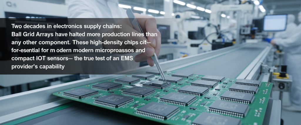

In the world of electronics manufacturing, a single microscopic defect can halt an entire production line. With over two decades of experience in PCBA (Printed Circuit Board Assembly), OminiPCBA knows that BGA (Ball Grid Array) components are often the primary cause of assembly delays. These high-density packages, essential for modern computing and smart devices, hide their connections beneath the silicon—making them the ultimate test of a manufacturer's technical capability.
Engineers favor BGAs for their high pin counts and space efficiency. However, for procurement teams, they represent a "black box" challenge. Unlike standard SMT or through-hole components, BGA solder joints are invisible to the naked eye. Ensuring quality requires specialized equipment and a rigorous control process.
Understanding the BGA "Black Box"
Instead of traditional leads, BGAs utilize tiny solder spheres on the underside of the component. During the reflow soldering process, these spheres melt to form electrical and mechanical bridges with the PCB pads. This hidden architecture introduces several critical manufacturing hurdles:
1. The "Popcorn Effect" (Moisture Sensitivity)
Plastic BGA packages are hygroscopic—they absorb moisture from the air. If these components are not stored or handled correctly, trapped moisture expands into steam during the 240°C reflow process. This internal pressure can crack the package, a defect known in the industry as "popcorning."
2. Precision Placement & Pitch Challenges
With pitches often dropping below 0.5mm, there is zero margin for error. Even a microscopic shift during the Pick and Place stage can lead to short circuits or open joints. Accuracy isn't just a metric; it is the fundamental requirement for functional hardware.
Critical Process Controls in China PCBA Assembly
When vetting a PCBA supplier in China (whether in tech hubs like Shenzhen or Suzhou), equipment is only half the story. The true value lies in their BGA process control. Here is what you should expect from a high-quality EMS partner:
I. The Baking Regime
At OminiPCBA, baking is a non-negotiable standard for all moisture-sensitive BGAs. We follow strict IPC/JEDEC standards to remove humidity before assembly. Pro Tip: Always ask your supplier for baking logs. If the documentation is missing, the quality of your batch is at risk.
II. Advanced Stencil Design & Solder Paste Printing
The integrity of a BGA joint starts with the stencil.
Aperture Design: Too large, and you risk solder bridging; too small, and you get "insufficient solder" leading to brittle joints.
Technology: For fine-pitch BGAs, we utilize electro-polished or nano-coated stencils. These specialized finishes ensure a clean release of solder paste, preventing "clogging" and ensuring consistent volume across thousands of pads.
III. Optimized Reflow Profiling
Soldering BGAs is where science meets craftsmanship. A "one-size-fits-all" thermal profile leads to failure.
Cold Solder Joints: Occur if the peak temperature is too low to fully melt the alloy.
Head-in-Pillow (HiP) Defects: Caused by excessive heat or uneven thermal expansion, where the BGA ball and the paste touch but do not fuse.
Omini’s Approach: We develop a custom thermal curve for every unique PCB design, ensuring even heat distribution and minimizing thermal stress on the components.
Inspection: Seeing the Unseen
Since BGA joints are hidden, OminiPCBA employs a multi-layered inspection strategy to guarantee 100% reliability.
Automated X-Ray Inspection (AXI)
This is the gold standard. If a factory claims to handle BGA assembly without X-ray capabilities, they cannot guarantee quality. Our X-ray systems detect:
Solder Voids: Identifying air pockets within the joint (kept strictly within IPC Class 2 or 3 limits).
Bridging: Spotting merged solder balls that cause shorts.
Misalignment: Ensuring the chip is perfectly centered on the pads.
Electrical & Functional Testing
While X-ray checks the structure, electrical tests verify performance:
ICT (In-Circuit Test): Ideal for high-volume production using a "bed of nails" fixture.
Flying Probe: Perfect for PCBA prototypes, offering high flexibility without custom fixtures.
Boundary Scan (JTAG): Using software to test digital BGA pins individually, ensuring every pathway is active.
The "Via-in-Pad" Solution
For high-density designs, traditional "dog-bone" routing often fails. OminiPCBA specializes in Via-in-Pad technology—drilling vias directly into the BGA pads, plating them, and filling them with epoxy/copper. This saves critical board space while maintaining signal integrity, though it requires precise cost-benefit planning during the quoting phase.
Why Partner with OminiPCBA?
Precision is our baseline. From automated X-ray inspection to climate-controlled component storage, OminiPCBA combines China’s manufacturing efficiency with world-class quality standards. Whether you are scaling a complex layout or building a high-speed prototype, we ensure your BGA assembly is flawless from the first solder ball to the final functional test.
Related Articles
Contacts
Email: sales@ominipcba.com
Mobile: +86-185-7640-5228
Copyright © 2007-2026. Omini Electronics Limited. All rights reserved.
Head Office: +86-755-2357-1819
Services
Your China turnkey partner for electronics manufacturing. We bridge design to delivery by leveraging the Shenzhen electronics ecosystem for precision engineering and streamlined PCBA supply chain logistics.
Ready to Build?
Get a comprehensive quote within 24 hours.
