Phone: +86-755-2357-1819 Mobile: +86-185-7640-5228 Email: sales@ominipcba.com whatsapp: +8618576405228

Blind Vias: A Sourcing Expert’s Guide to High-Density Interconnects
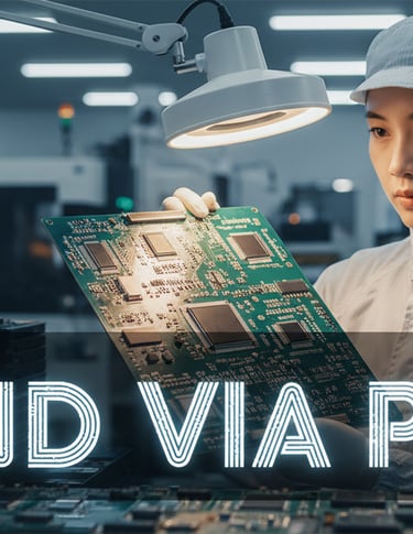
Unlock the potential of HDI designs with Blind Via PCBs. Learn how this technology reduces layer count and improves signal integrity in China PCB manufacturing
PCB TECHNOLOGYPCB MANUFACTURINGPCB ASSEMBLY
OminiPCBA
12/16/20253 min read

The relentless drive toward miniaturization is pushing the limits of traditional PCB layer stacking. Hardware engineers today face the dual challenge of increasing component density while procurement teams demand lower per-unit costs. In the modern electronics landscape, what happens inside the substrate is often more critical than the surface layout.
Enter the Blind Via.
With over two decades of supply chain expertise in Shenzhen’s PCB manufacturing hub, OminiPCBA has seen blind vias evolve from niche aerospace technology to a standard requirement for consumer electronics. However, blind vias are not a "magic bullet." Without a deep understanding of manufacturing constraints, they can unnecessarily inflate material costs. This guide outlines how to leverage blind via technology to optimize both performance and budget.
What is a Blind Via?
In traditional PCB manufacturing, a Through-Hole Via is drilled entirely through the board from top to bottom. While cost-effective, this method consumes valuable routing space on every single layer.
A Blind Via starts on a surface layer (top or bottom) but terminates at a specific internal layer without penetrating the entire board. When looking at the PCB, you will see the via opening on one side, but the opposite side remains solid. This "hidden" termination point is what gives the via its name.
This technology is the backbone of High-Density Interconnect (HDI) designs. By terminating vias early, designers free up "real estate" on the opposite side of the board for additional components or complex trace routing.
The Cost vs. Capability Trade-off
1. The Initial Investment
From a pure fabrication standpoint, blind vias are more expensive than through-holes. The process requires precision laser drilling or controlled-depth mechanical drilling, followed by specialized plating cycles. These extra steps increase the manufacturing lead time and the initial price per board.
2. The Total Cost of Ownership (TCO) Savings
While the unit price for a blind via board may be higher, the system-level costs often decrease. Here’s how:
Layer Reduction: We frequently see projects transition from a 12-layer through-hole design to an 8-layer HDI design using blind vias. Reducing the number of copper sheets and prepreg layers can offset the costs of laser drilling.
Increased Panelization: By shrinking the board footprint, you can fit more units onto a single production panel, significantly lowering the "cost per piece" in high-volume runs.
Enhanced Routing Efficiency: Blind vias allow for tighter spacing and more direct signal paths, reducing the need for complex, expensive substrate materials.
Key Applications for Blind Vias
Compact Consumer Tech: In smartphones and wearables, every square millimeter is vital. Blind vias prevent vias from interfering with component placement on the reverse side.
High-Pin-Count BGAs: For Fine-Pitch BGAs, blind vias allow designers to escape-route signals from the inner balls to internal layers without the need for "dog-bone" traces, clearing surface congestion.
Signal Integrity & High-Speed Data: By eliminating the "stub" (the unused portion of a through-hole), blind vias reduce signal reflections and impedance mismatches. This is critical for next-gen networking and high-frequency RF designs.
DFM (Design for Manufacturing) Tips for China-Based Production
To ensure your HDI design is optimized for a Chinese PCBA manufacturer like OminiPCBA, follow these guidelines:
1. Optimize the Aspect Ratio
For reliable plating, maintain a via depth-to-diameter ratio of 0.8:1 or 1:1. If a hole is too deep and narrow, the plating chemistry cannot flow effectively, leading to potential voids and field failures. Keep blind vias "shallow," typically spanning only one or two dielectric layers.
2. Material Selection
Not all FR4 is created equal. High glass-content materials can result in "ragged" holes when laser-drilled. Work with OminiPCBA to select Laser-Drillable Prepreg that ensures clean hole walls and robust electrical connections.
3. Maintain Stack-up Symmetry
Complex HDI designs are prone to warping during the reflow process. Ensure your layer stack-up is symmetrical to balance internal stresses, especially when mixing rigid and flexible substrates.
Precision Assembly for HDI
While blind vias are "hidden" during the SMT (Surface Mount Technology) process, they enable much tighter component densities. As spacing shrinks, the need for precision increases. OminiPCBA utilizes high-accuracy placement equipment capable of handling 0201 and 01005 components with repeatable reliability.
Partner with OminiPCBA for Your Next HDI Project
Navigating the complexities of HDI and blind via technology requires a partner who understands the nuance of laser buildup and sequential lamination. Based in the heart of Shenzhen, OminiPCBA combines the speed of Chinese manufacturing with rigorous engineering oversight. We provide thorough DFM reviews before production to eliminate guesswork and ensure your design is ready for the real world.
Ready to shrink your footprint and optimize your costs? Contact OminiPCBA today.
Related Articles
Contacts
Email: sales@ominipcba.com
Mobile: +86-185-7640-5228
Copyright © 2007-2026. Omini Electronics Limited. All rights reserved.
Head Office: +86-755-2357-1819
Services
Your China turnkey partner for electronics manufacturing. We bridge design to delivery by leveraging the Shenzhen electronics ecosystem for precision engineering and streamlined PCBA supply chain logistics.
Ready to Build?
Get a comprehensive quote within 24 hours.
