Phone: +86-755-2357-1819 Mobile: +86-185-7640-5228 Email: sales@ominipcba.com whatsapp: +8618576405228

The Hardware Engineer’s Guide to PCB Layout: Components, Traces, and Ground Planes
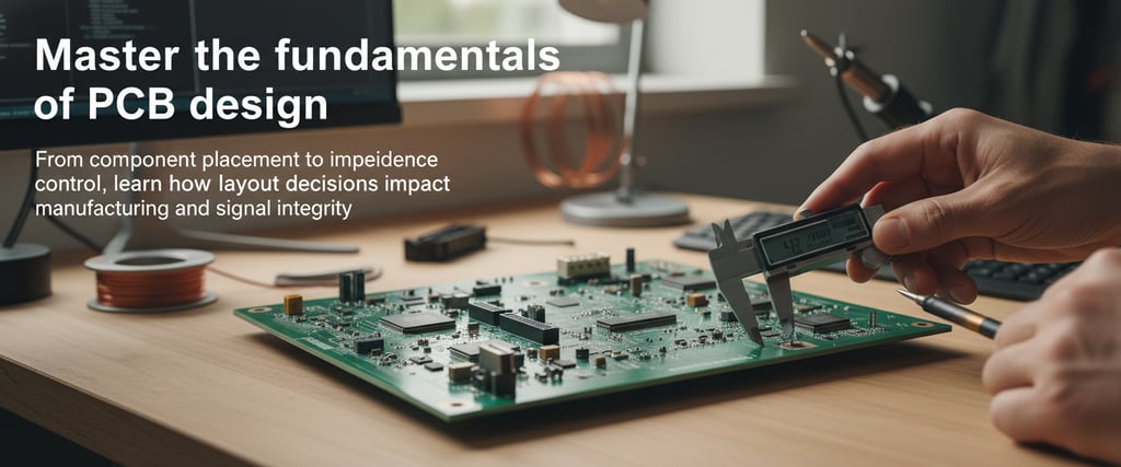
Master the fundamentals of PCB design. From component placement to impedance control, learn how layout decisions impact manufacturing and signal integrity
PCB MATERIALS
Amanda
12/8/20253 min read

A Printed Circuit Board (PCB) is more than a foundation for components; it is the physical execution of your circuit theory. While EDA tools simplify routing, the precision of your layout determines whether a board becomes a high-performance product or a costly failure.
As senior engineers, we often see designs fail not due to schematic errors, but because of poor layout decisions. Issues like signal integrity (SI) degradation, thermal hotspots, and assembly defects are often locked in long before the files reach the PCB manufacturing stage. Mastering the interplay between components, traces, and ground planes is the only way to ensure a robust, reliable design.
Strategic Component Placement
Placement is the most critical phase of PCB layout best practices. Once a board is fabricated, relocating a chip to solve noise issues is impossible. Effective placement requires balancing several technical factors:
Logic-Driven Signal Flow: Components should follow the schematic’s logical flow. Position connectors at the board edge, followed by protection circuitry, power regulators, and then the MCU or processors. Grouping related components—such as placing decoupling capacitors immediately adjacent to IC power pins—is non-negotiable for signal stability.
Thermal Management: High-power MOSFETs, processors, and regulators generate significant heat. Overcrowding these components without considering airflow or thermal relief creates hotspots that degrade performance. Use thermal vias to transfer heat to internal ground planes.
Design for Manufacturability (DFM): To optimize PCBA assembly, place SMT components on a single side to reduce reflow cycles. Ensure proper clearance for pick-and-place nozzles and manual rework. A board that is impossible to service is a design failure.
High-Performance Trace Routing
Traces are the "veins" of your PCB. Their geometry directly dictates signal quality and power distribution.
Impedance Control & Signal Integrity: For high-speed digital designs, traces act as transmission lines. You must control characteristic impedance (typically 50Ω single-ended) by calculating trace width relative to your PCB stack-up. To minimize crosstalk, avoid running sensitive analog traces parallel to high-speed clock lines.
Power Distribution: Trace width must be sized for current capacity. A narrow trace under high load acts as a fuse. For high-current paths, utilize copper pours and polygons rather than thin traces to minimize voltage drop and heat rise.
Ground Planes: The Foundation of EMI Control
The ground plane is the return path for every signal. Mastering its topology is essential for EMC/EMI compliance.
The Return Path: High-frequency currents follow the path of least inductance, which is directly beneath the signal trace. Breaking the ground plane under a high-speed line creates a "loop antenna," radiating Electromagnetic Interference (EMI) and ruining signal integrity.
Ground Stitching: In multi-layer boards, use via stitching to connect ground pours across layers. This reduces ground impedance and provides a Faraday cage effect, shielding sensitive internal signals from external noise.
Mixed-Signal Grounding: In designs featuring both analog and digital circuits, isolation is key. Use star grounding to connect disparate grounds at a single point, preventing digital switching noise from corrupting sensitive analog signals.
Beyond Rigid: Rigid-Flex Design
For complex mechanical form factors, Rigid-Flex PCB layouts require specialized rules:
Traces must run perpendicular to the bend line to prevent copper cracking.
Avoid placing vias or components in flexible regions.
Use hatched ground planes to maintain flexibility without sacrificing shielding.
Optimize Your Production with OminiPCBA
Navigating the complexities of layout, fabrication, and PCBA assembly requires a partner with deep technical expertise. At Omini, we provide a comprehensive Design for Manufacturing (DFM) review, optimizing your files for yield and performance.
From simple IoT sensors to complex high-speed controllers, we ensure your layout translates perfectly into a finished product. Partner with Omini for precision PCB manufacturing and assembly.
Related Articles
Contacts
Email: sales@ominipcba.com
Mobile: +86-185-7640-5228
Copyright © 2007-2026. Omini Electronics Limited. All rights reserved.
Head Office: +86-755-2357-1819
Services
Your China turnkey partner for electronics manufacturing. We bridge design to delivery by leveraging the Shenzhen electronics ecosystem for precision engineering and streamlined PCBA supply chain logistics.
Ready to Build?
Get a comprehensive quote within 24 hours.
