Phone: +86-755-2357-1819 Mobile: +86-185-7640-5228 Email: sales@ominipcba.com whatsapp: +8618576405228

Mastering PCB Miniaturization: HDI, mSAP & 008004 Assembly Design
Overcome the physical limits of high-density interconnects. Analyze the fabrication and SMT challenges of 008004 components, mSAP traces, and ELIC stacking.
PCB TECHNOLOGYPCB MANUFACTURINGPCB ASSEMBLY
OminiPCBA
1/1/20263 min read
Modern electronics demand a radical paradox: higher performance within shrinking footprints. As gadgets become more compact, the printed circuit board has evolved from a simple component carrier into a complex 3D interconnect network. Today’s engineers must look beyond traditional design rules, facing a reality where material science, physics, and manufacturing constraints converge at the microscopic level.
At the leading edge of HDI (High-Density Interconnect) technology, the boundary between semiconductor packaging and PCB fabrication has blurred. Features once reserved for silicon are now integrated into the substrate, requiring sub-micron precision. Every element of the signal path—from copper grain structures to solder paste rheology—requires a fundamental shift in manufacturing philosophy.
Precision Trace Geometry: Moving Beyond 30 Microns
Traditional subtractive etching, which removes copper to define circuits, reaches its physical limit at approximately 40µm. At this scale, chemical etchants cause "undercutting," where the acid eats away the sidewalls of the trace, resulting in a trapezoidal cross-section. This uneven geometry increases electrical resistance and compromises signal integrity in high-frequency applications.
To support the next generation of medical wearables and IoT devices, OminiPCBA utilizes mSAP (modified Semi-Additive Process). This technique builds circuitry from the ground up:
Additive Construction: Copper is electroplated into ultra-fine patterns defined by high-resolution photoresist.
Vertical Sidewalls: mSAP produces rectangular trace profiles down to 20µm, ensuring consistent impedance and superior electrical performance.
Enhanced Adhesion: Advanced molecular bonding ensures fine-line traces remain structurally sound despite their minimal surface area.
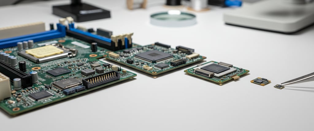
The 008004 Component Revolution
The roadmap of passive component downsizing has moved from 0402 to 0201, 01005, and now the 008004 (0.25mm x 0.125mm) reality. These components are nearly invisible to the naked eye, presenting significant challenges for high-speed SMT (Surface Mount Technology) assembly.
Successful 008004 integration requires mastering Surface Tension Management:
Tombstoning Prevention: Precise thermal profiling is critical to prevent uneven solder wetting, which can flip or misalign these microscopic parts.
Solder Paste Innovation: Standard Type 4 powder is too coarse for 008004 apertures. We utilize Type 5 and Type 6 fine-grain powders (5–15µm) combined with nano-coated stencils to ensure perfect paste release and zero bridging.
Z-Axis Integration: ELIC and Stacked Microvias
When X-Y real estate is exhausted, the only direction left is up. ELIC (Every Layer Interconnect) technology allows for Any-Layer HDI designs, replacing space-consuming through-holes with stacked, copper-filled microvias.
Vertical Routing: ELIC enables a continuous copper column through any layer, freeing up routing channels and increasing connection density.
Reliability Engineering: Because stacked microvias are susceptible to vertical thermal expansion stress, OminiPCBA employs rigorous plating controls and oxygen-free environments to prevent interface delamination during reflow.
Rigid-Flex Architecture for 3D Spatial Optimization
Miniaturization often involves conforming electronics to ergonomic, non-linear enclosures. Rigid-flex PCBs eliminate bulky connectors and wire harnesses by integrating flexible polyimide sections directly into the circuit.
Neutral Axis Theory: We design layouts so that conductive layers sit at the center of the bend radius, minimizing mechanical fatigue.
Assembly Support: To counter the inherent instability of flexible materials during SMT, we use custom-engineered carriers to ensure flat-plane precision during printing and component placement.
Thermal Management in High-Density Designs
Packing high-power components into small volumes creates localized heat sinks that can degrade battery life or throttle performance. OminiPCBA implements advanced thermal solutions:
VIPPO (Via-In-Pad Plated Over): Copper-filled vias situated directly under component pads pull heat to internal ground planes.
Copper Inlays: For extreme thermal loads, solid copper coins are integrated into the substrate to provide a direct path for heat dissipation.
Signal Integrity and "The Untestable"
In crowded layouts, Crosstalk and the Glass Weave Effect become dominant threats. We mitigate these through:
Tight Coupling: Using ultra-thin dielectrics to bring signal lines closer to return planes.
Spread Glass Weave: Utilizing specialized laminates to ensure uniform signal velocity across high-speed differential pairs.
As test points disappear to save space, we transition from physical "bed-of-nails" testing to Advanced Functional Validation:
Boundary Scan (JTAG): Software-driven testing of interconnects.
3D AXI (Automated X-Ray Inspection): Utilizing Computed Tomography to visualize hidden solder joints under BGAs and CSPs, ensuring void-free connections where the human eye cannot reach.
The Future of PCBA Partnership
At OminiPCBA, we believe shrinking a design is not a linear process—it is a holistic one. Success at the 15µm level requires a tight feedback loop between design and the factory floor. By controlling every micron of solder mask and every degree of the thermal profile, we turn the most ambitious miniaturization concepts into reliable, mass-produced reality.
Related Articles
Contacts
Email: sales@ominipcba.com
Mobile: +86-185-7640-5228
Copyright © 2007-2026. Omini Electronics Limited. All rights reserved.
Head Office: +86-755-2357-1819
Services
Your China turnkey partner for electronics manufacturing. We bridge design to delivery by leveraging the Shenzhen electronics ecosystem for precision engineering and streamlined PCBA supply chain logistics.
Ready to Build?
Get a comprehensive quote within 24 hours.
