Phone: +86-755-2357-1819 Mobile: +86-185-7640-5228 Email: sales@ominipcba.com whatsapp: +8618576405228


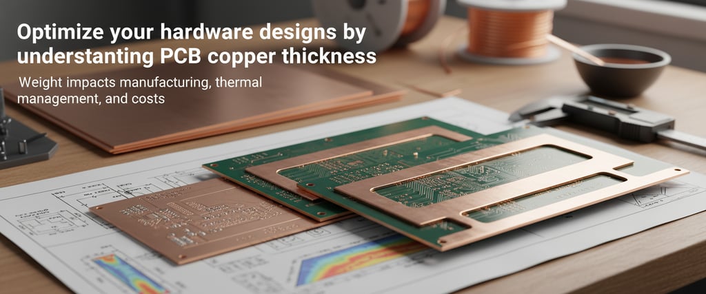
PCB Copper Thickness: A Practical Guide for Your Board's Performance
A hardware engineer's guide to PCB copper thickness. Learn how to choose the right weight for current, thermal, and impedance needs in your PCB manufacturing process.
PCB MANUFACTURING
Amanda
12/1/20243 min read
If you’ve ever opened your EDA tool and reflexively accepted the default 1 oz copper setting, you aren’t alone. For standard digital designs, that baseline works. However, as a veteran engineer who has seen countless boards fail due to thermal runaway or poor manufacturing yields, I can tell you that copper weight is a critical variable. It must be actively managed—not just for signal integrity, but for PCB manufacturability (DFM) and total project cost.
Whether you are a layout engineer optimizing a power rail or a procurement manager analyzing a Bill of Materials (BOM), understanding the nuances of copper thickness is essential for a reliable build.
Decoding the "Ounce" in PCB Stack-Ups
In the electronics industry, we uniquely measure copper thickness by weight. When we specify "1 oz copper," we are referring to one ounce of copper rolled out evenly over a surface area of one square foot.
In a practical PCB stack-up, these values translate to:
0.5 oz ≈ 0.7 mils (17.5 µm)
1 oz ≈ 1.37 mils (35 µm)
2 oz ≈ 2.8 mils (70 µm)
While 1 oz is the industry workhorse—balancing cost, etching precision, and current-carrying capacity—it is not a universal solution.
When to Go Heavy: High Current and Thermal Management
The primary driver for increasing copper weight is current handling. In power supplies, motor controllers, or EV charging modules, standard 1 oz traces can act as unintentional fuses.
Heavy copper (2 oz, 3 oz, or higher) reduces DC resistance, minimizing voltage drops and heat generation. It essentially turns your PCB into a heatsink, spreading thermal loads across the substrate. However, this shift impacts PCBA assembly.
During reflow or hand-soldering, heavy copper acts as a massive heat sink, pulling energy away from the joint. This makes the SMT vs. through-hole debate critical; achieving a proper solder fillet on a heavy-copper PTH (Plated Through-Hole) requires significantly more thermal energy. Without precise thermal profiling, you risk cold solder joints and intermittent failures.
When to Stay Thin: Fine Pitch and Flexibility
More copper isn't always better. If you are designing a rigid-flex PCB or a board subject to high mechanical stress, thinner copper (0.5 oz) is superior. It is more ductile, reducing the risk of trace cracking during bending.
From a DFM (Design for Manufacturability) perspective, heavy copper limits your layout density. The chemical etching process causes "undercutting"—where the etchant eats away at the side of a trace as it bites downward.
Fine-pitch BGAs and 0201 components require high-precision etching.
Heavy copper makes tight trace/space tolerances impossible to maintain.
If your design requires high density, stick to standard or thin copper to ensure the layout is printable and repeatable.
PCB Layout Best Practices for Copper Weight
To ensure your design survives the fabrication house and the test bench, follow these professional layout guidelines:
Calculate, Don’t Guess: Use IPC-2152 or IPC-2221 standards to determine the required trace width based on your target current and allowable temperature rise.
Increase Clearances: If you specify 2 oz copper, you must increase your spacing. A reliable rule of thumb is an 8-mil minimum space for 2 oz copper, compared to the 4–5 mils possible with 1 oz.
Prioritize Thermal Reliefs: For heavy copper layers, always use thermal relief spokes on ground pads. Without them, heat dissipates too quickly during assembly, leading to "tombstoning" or poor solder wetting.
Balance the Stack-Up: Maintain symmetry in your copper weights (e.g., if Layer 1 is 2 oz, Layer 4 should also be 2 oz). Asymmetrical copper distribution causes PCB warping or bowing during the high temperatures of the reflow oven.
The Procurement Angle: Cost vs. Performance
For procurement managers: thicker copper carries a premium. It involves higher raw material costs, longer etching times, and more complex lamination cycles.
However, investing in a robust bare board can reduce your total BOM cost by eliminating the need for bulky external heatsinks or cooling fans. It is a strategic trade-off that engineering and purchasing must evaluate in tandem.
Partner with OminiPCBA for Your Next Build
Choosing the right copper weight is a pivotal design decision. At OminiPCBA, we bridge the gap between complex engineering requirements and manufacturing reality. From high-power heavy copper boards to high-density interconnect (HDI) and rigid-flex designs, our team provides comprehensive layout reviews and turnkey assembly.
Related Articles
Contacts
Email: sales@ominipcba.com
Mobile: +86-185-7640-5228
Copyright © 2007-2026. Omini Electronics Limited. All rights reserved.
Head Office: +86-755-2357-1819
Services
Your China turnkey partner for electronics manufacturing. We bridge design to delivery by leveraging the Shenzhen electronics ecosystem for precision engineering and streamlined PCBA supply chain logistics.
Ready to Build?
Get a comprehensive quote within 24 hours.
