Phone: +86-755-2357-1819 Mobile: +86-185-7640-5228 Email: sales@ominipcba.com whatsapp: +8618576405228

Strategic PCB Manufacturer Selection & Failure Prevention
Master hardware reliability. A technical deep dive into selecting manufacturing partners, analyzing PCB failure modes, and optimizing PCBA production yields.
PCB TECHNOLOGYPCB MANUFACTURINGPCB ASSEMBLY
OminiPCBA
2/13/20265 min read
Moving from a tested model to a finished electronics item often trips up because of unseen issues that might wreck the whole development plan. Picking who makes your device isn’t just about price - it shapes how well the gadget holds up over time. When even a tiny break in a circuit line can cause major problems later, choosing between a cheap builder and one that meets high standards decides everything.
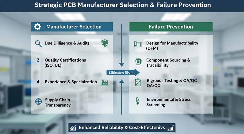
The Architecture of Selection Beyond the Quote
Chasing the lowest price for a blank circuit board might seem smart at first glance. Yet what really adds up are the unseen costs - fixing mistakes, scrapped units, even field failures down the line. Smart sourcing looks beyond the initial quote. Think about how well a contract manufacturer handles quality behind the scenes. Their skill in reading intricate designs can make or break long-term reliability. True value hides in processes most overlook. Only later do people notice the difference.
What a shop can actually do often shows up when production heats up. Take 3-mil traces - lots of places say they can print them, but doing it cleanly on every board in a batch of five hundred? That takes sharp LDI tools and etch baths that behave. Engineers tend to look at how well the solder mask lines up. They also check if copper builds evenly inside narrow holes, run after run. Precision doesn’t shout. It just stays steady.
Engineering Support and the DFM Feedback Loop
It's what sets apart top-tier manufacturers - having a solid plan built right into the design phase. Not just putting parts together exactly as drawn. Think of them more like quality gatekeepers, spotting hiccups long before any machine starts cutting. Catching things such as gaps between pads being way too narrow. Seeing when tiny parts sit dangerously near the edge, messing up clean breaks later. Even adjusting how copper connects during cooling so nothing warps under heat.
Early teamwork shines in top factories, like those measured against Ominipcbas standards. With smart software simulating how parts go together, builders spot trouble spots - say, solder links forming too close on tiny BGAs or uneven heating that flips small parts upright during cooking. Acting ahead turns the builder into more than just a vendor - they become part of the design crew, working shoulder to shoulder. Instead of waiting for problems, they shape solutions before metal ever heats up.
Analyzing Why PCBS Fail
When things break, it is often not about one moment. What matters most hides inside how materials wear down over time. Instead of blaming sudden issues, look closer at slow shifts like trapped chemicals or tiny cracks growing beneath surfaces. Most problems start small, building quietly until something finally gives way.
Temperature Changes Cause Material Expansion Differences
Heat makes materials grow, yet they do not always stretch equally. A circuit board combines resin, glass fibers, copper - each reacting differently when warmed by solder ovens or power-heavy parts. When layers push outward too much along the thickness direction, tiny cracks form inside drilled holes if the copper cannot bend far enough. These fractures cause broken paths that slip past routine checks but die fast once used outside. Mismatched swelling hides quietly until real conditions expose it.
Ionic Contamination and Electrochemical Migration
Tiny bits of dirt matter more when gadgets work in damp or tough conditions. Without proper cleaning steps, leftover chemicals stick around after manufacturing finishes. Voltage plus wetness helps those leftovers turn into charged particles that spread out slowly. Like thin wires made by nature, sharp metal strands stretch along insulating layers over time. When they bridge gaps meant to block current, sparks may follow - sometimes heat, sometimes total breakdown follows close behind.
Precision in SMT Processes
Inside every electronics factory, tiny connections take shape on the SMT line - this spot matters more than most. Getting it right leans heavily on how well solder paste sticks at first. Then comes positioning; parts must land exactly where they belong, not a millimeter off. After that, heat enters slowly, shaping bonds without burning anything up. Each step feeds into the next like links in a chain nobody sees.
Most problems on the board start during paste application. Machines that print solder get checked by 3D scanners. Every tiny blob gets measured - its shape, its thickness. Too little paste weakens joints. Too much links pins that should stay apart. Precision matters most where connections sit close together. Strong bonds need just the right amount. Errors here spread down the line.
Getting the heating process right matters. Not every circuit board heats up the same way. Some parts suck up warmth fast, others barely notice it. Big metal patches behave unlike tiny pieces when warmed. Smart makers check real temperatures using sensor tools placed like hidden scouts. These show exactly how hot things get during cooking. That helps adjust warm-up time and top heat carefully. Too much too fast cracks fragile chips. Too little leaves weak links behind. Balance keeps everything strong without stress.
The Role of Advanced Inspection X Ray and AOI
Hidden connections beneath BGA and QFN chips make basic visual checks useless today. That’s when 3D AOI steps in - backed by X-ray imaging - to catch what eyes can’t see.
Seeing inside parts is possible when engineers use X-ray checks on solder ball connections. Because trapped gases escape during heating, tiny empty spaces might form inside BGA spheres - these shrink the metal contact zone. When that happens, electrical flow meets more pushback while shaking forces raise the risk of cracks later. At places such as Ominipcba, scanning with X-rays becomes routine for complicated circuit panels so hidden sections match surface quality in trustworthiness.
Choosing Materials and Keeping Layers Strong
Picking the right base stuff - like FR4, Rogers, or Polyimide - shapes how the board handles electric and physical stress. When signals move fast, what matters is how steady the material keeps its Df and Dk as frequency shifts. Lower-cost layers tend to show a weave issue: glass threads inside can twist timing between paired signals.
Flat surfaces matter most when placing tiny parts. Yet even small flaws hide beneath gold layers if nickel mixes go wrong. Instead of skipping checks, some factories treat chemistry like machine tools - precise every time. While HASL suits rough conditions, smooth finishes demand tighter control. Each choice ties directly to where the board will live and work. Mistakes in baths lead to brittle joints no test can fix later.
Strategic Testing: ICT vs. FCT
Fault-free production depends on multiple test layers. Starting with the basics, In-Circuit Testing examines the bare structure - spotting broken connections, unintended links, or wrong parts. Yet despite catching physical flaws, it won’t confirm if the circuit actually works right.
Testing how devices work starts by copying normal usage conditions. Power flows in, signals follow, checking if chips talk right and voltage holds steady when stressed. One method checks steps inside production. Another confirms overall behavior works as intended. Together they form layers that catch problems before products leave the factory. Units that fail never make it to buyers.
Tracking Goods Across Supply Chains
When parts are hard to find or fake ones pop up, how a company buys its components becomes crucial. From the moment a chip lands on a circuit board, it can be tracked to exactly which batch and when it was made, thanks to solid tracking tools. Suppose one type of capacitor starts failing often; a well-equipped site then spots each device already sent out with that part - fast. That precision means only affected units get pulled, avoiding wide-scale takebacks full of cost and hassle.
The Way to Better Hardware
Picking a solid PCB maker means valuing skill more than just cutting costs. Not every step adds up the same - design checks, precise component placement, careful review throughout production shape what comes out. Hardware survives tough conditions when problems like heat shifts or chemical residue get addressed early, right where it's built. Some teams see building circuits as exact work, not something picked off a shelf - the way Omnipcb does, for example - and that steadiness helps new tech grow without surprise flaws. Decisions made on the factory floor echo later in performance, far beyond initial price tags.
Related Articles
Contacts
Email: sales@ominipcba.com
Mobile: +86-185-7640-5228
Copyright © 2007-2026. Omini Electronics Limited. All rights reserved.
Head Office: +86-755-2357-1819
Services
Your China turnkey partner for electronics manufacturing. We bridge design to delivery by leveraging the Shenzhen electronics ecosystem for precision engineering and streamlined PCBA supply chain logistics.
Ready to Build?
Get a comprehensive quote within 24 hours.
